- 您现在的位置:买卖IC网 > Sheet目录114587 > 552CC000230BGR (SILICON LABORATORIES) VCXO, CLOCK, 24.576 MHz, CMOS OUTPUT
Si552
Rev. 0.5
3
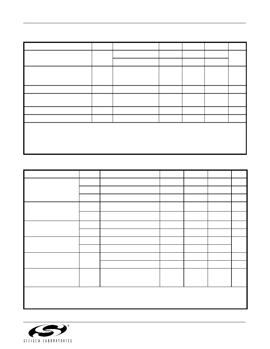
Table 3. CLK± Output Frequency Characteristics
Parameter
Symbol
Test Condition
Min
Typ
Max
Units
Nominal Frequency1,2,3
fO
LVDS/CML/LVPECL
10
—
945
MHz
CMOS
10
—
160
Temperature Stability1,4
f/fO
TA = –40 to +85 C
–20
–50
–100
—
+20
+50
+100
ppm
Absolute Pull Range1,4
APR
±25
—
±150
ppm
Aging
Frequency drift over
15 year life.
——
±10
ppm
Power up Time5
tOSC
——
10
ms
Settling Time After FS Change
tFRQ
——
10
ms
Notes:
1. See Section 3. "Ordering Information" on page 7 for further details.
2. Specified at time of order by part number. Also available in frequencies from 970 to 1134 MHz and 1213 to 1417 MHz.
3. Nominal output frequency set by VCNOM =3/8 xVDD.
4. Selectable parameter specified by part number.
5. Time from power up or tristate mode to fO (to within ±1 ppm of fO).
Table 4. CLK± Output Levels and Symmetry
Parameter
Symbol
Test Condition
Min
Typ
Max
Units
LVPECL Output Option1
VO
mid-level
VDD – 1.42
—
VDD – 1.25
V
VOD
swing (diff)
1.1
—
1.9
VPP
VSE
swing (single-ended)
0.5
—
0.93
VPP
LVDS Output Option2
VO
mid-level
1.125
1.20
1.275
V
VOD
swing (diff)
0.32
0.40
0.50
VPP
CML Output Option2
VO
mid-level
—
VDD – 0.75
—
V
VOD
swing (diff)
0.70
0.95
1.20
VPP
CMOS Output Option3
VOH
IOH =32mA
0.8 x VDD
—
VDD
V
VOL
IOL =32mA
——
0.4
Rise/Fall time (20/80%)
tR, tF
LVPECL/LVDS/CML
—
350
ps
CMOS with CL = 15 pF
—
1
—
ns
Symmetry (duty cycle)
SYM
LVPECL:
VDD – 1.3 V (diff)
LVDS:
1.25 V (diff)
CMOS:
VDD/2
45
—
55
%
Notes:
1. 50
to VDD – 2.0 V.
2. Rterm = 100 (differential).
3. CL = 15 pF
发布紧急采购,3分钟左右您将得到回复。
相关PDF资料
552AD000127BG
VCXO, CLOCK, 693.48299 MHz, LVPECL OUTPUT
550AC250M000BGR
VCXO, CLOCK, 250 MHz, LVPECL OUTPUT
550AD669M327BGR
VCXO, CLOCK, 669.327 MHz, LVPECL OUTPUT
552AC000189BGR
VCXO, CLOCK, 126.2 MHz, LVPECL OUTPUT
554CD000010BGR
VCXO, CLOCK, 108 MHz, CMOS OUTPUT
554CD000110BGR
VCXO, CLOCK, 108 MHz, CMOS OUTPUT
550AD216M000BGR
VCXO, CLOCK, 216 MHz, LVPECL OUTPUT
554MD000244BG
VCXO, CLOCK, 166.6286 MHz, LVPECL OUTPUT
相关代理商/技术参数
552CC000230DG
功能描述:VCXO振荡器 DUAL VCXO 6 PIN 0.5PS RS JTR RoHS:否 制造商:Fox 封装 / 箱体:5 mm x 3.2 mm 频率:19.2 Mhz 频率稳定性:2.5 PPM 输出格式: 封装:Reel 电源电压:3 V 端接类型:SMD/SMT 尺寸:3.2 mm W x 5 mm L x 1.5 mm H 最小工作温度:- 20 C 最大工作温度:+ 75 C
552CC000353DG
功能描述:VCXO振荡器 DUAL VCXO 6PIN .5ps RMS jitter RoHS:否 制造商:Fox 封装 / 箱体:5 mm x 3.2 mm 频率:19.2 Mhz 频率稳定性:2.5 PPM 输出格式: 封装:Reel 电源电压:3 V 端接类型:SMD/SMT 尺寸:3.2 mm W x 5 mm L x 1.5 mm H 最小工作温度:- 20 C 最大工作温度:+ 75 C
552CC000432DG
功能描述:VCXO振荡器 DUAL VCXO 6PIN .5ps RMS jitter RoHS:否 制造商:Fox 封装 / 箱体:5 mm x 3.2 mm 频率:19.2 Mhz 频率稳定性:2.5 PPM 输出格式: 封装:Reel 电源电压:3 V 端接类型:SMD/SMT 尺寸:3.2 mm W x 5 mm L x 1.5 mm H 最小工作温度:- 20 C 最大工作温度:+ 75 C
552CC622M080BG
制造商:SILABS 制造商全称:SILABS 功能描述:DUAL FREQUENCY VCXO (10 MHZ TO 1.4 GHZ)
552CC622M080BGR
制造商:SILABS 制造商全称:SILABS 功能描述:DUAL FREQUENCY VCXO (10 MHZ TO 1.4 GHZ)
552CD000109DG
制造商:Silicon Laboratories Inc 功能描述:CNTRLD OSC 74.175824MHZ/74.25MHZ VCXO CMOS 6PIN - Trays
552CD000131DG
制造商:Silicon Laboratories Inc 功能描述:OSCILLATOR - Trays
552CD000131DGR
制造商:Silicon Laboratories Inc 功能描述:OSCILLATOR - Tape and Reel